- 您现在的位置:买卖IC网 > Sheet目录3890 > PIC16C765T-I/L (Microchip Technology)IC MCU OTP 8KX14 USB 44PLCC
PIC16C745/765
DS41124C-page 134
Preliminary
2000 Microchip Technology Inc.
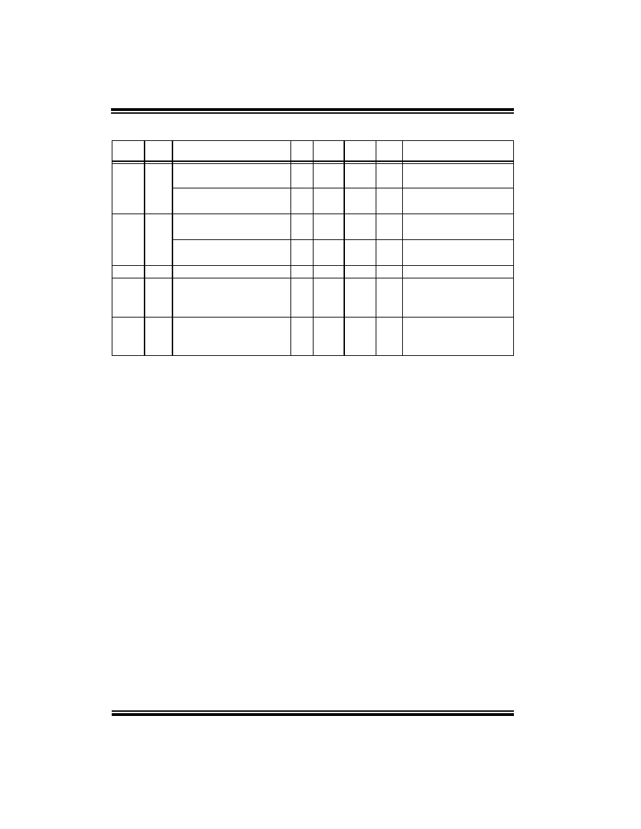
TABLE 16-2:
EXTERNAL CLOCK TIMING REQUIREMENTS
Param
No.
Sym
Characteristic
Min
Typ
Max
Units
Conditions
1A
FOSC
External CLKIN Frequency
(Note 1)
24
—
24
MHz
EC osc mode
6
—
6
MHz
E4 osc mode
Oscillator Frequency
(Note 1)
24
—
24
MHz
HS osc mode
6
—
6
MHz
H4 osc mode
1TOSC
External CLKIN Period
(Note 1)
41
—
41
ns
EC osc modes
167
—
167
ns
E4 osc mode
Oscillator Period
(Note 1)
41
—
41
ns
HS osc modes
167
—
167
ns
H4 osc mode
2TCY
Instruction Cycle Time (Note 1)
167
—
DC
ns
TCY = 4/FINT
3*
TOSL,
TOSH
External Clock in (OSC1) High or Low
Time
10
——
ns
EC oscillator
4*
TOSR,
TOSF
External Clock in (OSC1) Rise or Fall
Time
——
15
ns
EC oscillator
* These parameters are characterized but not tested.
Data in “Typ” column is at 5V, 25°C unless otherwise stated. These parameters are for design guidance only and are not
tested.
Note 1:
Instruction cycle period (TCY) equals four times the input oscillator time-base period when the PLL is enabled, or the input
oscillator time-base period divided by 4 when the PLL is disabled. All specified values are based on characterization data
for that particular oscillator type under standard operating conditions with the device executing code. Exceeding these
specified limits may result in an unstable oscillator operation and/or higher than expected current consumption. All devices
are tested to operate at “min.” values with an external clock applied to the OSC1/CLKIN pin. When an external clock input
is used, the “Max.” cycle time limit is “DC” (no clock) for all devices.
745cov.book Page 134 Wednesday, August 2, 2000 8:24 AM
发布紧急采购,3分钟左右您将得到回复。
相关PDF资料
PIC18C442T-E/L
IC MCU OTP 8KX16 A/D 44PLCC
PIC16C621A-40/SS
IC MCU OTP 1KX14 COMP 20SSOP
PIC16C622A-40/SS
IC MCU OTP 2KX14 COMP 20SSOP
PIC16CE623-30/SO
IC MCU OTP 512X14 EE COMP 18SOIC
PIC16CE624-30/SO
IC MCU OTP 1KX14 EE COMP 18SOIC
PIC16CE624-30/SS
IC MCU OTP 1KX14 EE COMP 20SSOP
PIC16CE623-30/SS
IC MCU OTP 512X14 EE COMP 20SSOP
PIC16CE624-30/P
IC MCU OTP 1KX14 EE COMP 18DIP
相关代理商/技术参数
PIC16C765T-I/PT
功能描述:8位微控制器 -MCU 14KB 256 RAM 33 I/O RoHS:否 制造商:Silicon Labs 核心:8051 处理器系列:C8051F39x 数据总线宽度:8 bit 最大时钟频率:50 MHz 程序存储器大小:16 KB 数据 RAM 大小:1 KB 片上 ADC:Yes 工作电源电压:1.8 V to 3.6 V 工作温度范围:- 40 C to + 105 C 封装 / 箱体:QFN-20 安装风格:SMD/SMT
PIC16C76T-04/SO
功能描述:8位微控制器 -MCU 14KB 368 RAM 22 I/O RoHS:否 制造商:Silicon Labs 核心:8051 处理器系列:C8051F39x 数据总线宽度:8 bit 最大时钟频率:50 MHz 程序存储器大小:16 KB 数据 RAM 大小:1 KB 片上 ADC:Yes 工作电源电压:1.8 V to 3.6 V 工作温度范围:- 40 C to + 105 C 封装 / 箱体:QFN-20 安装风格:SMD/SMT
PIC16C76T-04E/SO
功能描述:8位微控制器 -MCU 14KB 368 RAM 22 I/O RoHS:否 制造商:Silicon Labs 核心:8051 处理器系列:C8051F39x 数据总线宽度:8 bit 最大时钟频率:50 MHz 程序存储器大小:16 KB 数据 RAM 大小:1 KB 片上 ADC:Yes 工作电源电压:1.8 V to 3.6 V 工作温度范围:- 40 C to + 105 C 封装 / 箱体:QFN-20 安装风格:SMD/SMT
PIC16C76T-04I/SO
功能描述:8位微控制器 -MCU 14KB 368 RAM 22 I/O RoHS:否 制造商:Silicon Labs 核心:8051 处理器系列:C8051F39x 数据总线宽度:8 bit 最大时钟频率:50 MHz 程序存储器大小:16 KB 数据 RAM 大小:1 KB 片上 ADC:Yes 工作电源电压:1.8 V to 3.6 V 工作温度范围:- 40 C to + 105 C 封装 / 箱体:QFN-20 安装风格:SMD/SMT
PIC16C76T-10/SO
功能描述:8位微控制器 -MCU 14KB 368 RAM 22 I/O RoHS:否 制造商:Silicon Labs 核心:8051 处理器系列:C8051F39x 数据总线宽度:8 bit 最大时钟频率:50 MHz 程序存储器大小:16 KB 数据 RAM 大小:1 KB 片上 ADC:Yes 工作电源电压:1.8 V to 3.6 V 工作温度范围:- 40 C to + 105 C 封装 / 箱体:QFN-20 安装风格:SMD/SMT
PIC16C76T-10E/SO
功能描述:8位微控制器 -MCU 14KB 368 RAM 22 I/O RoHS:否 制造商:Silicon Labs 核心:8051 处理器系列:C8051F39x 数据总线宽度:8 bit 最大时钟频率:50 MHz 程序存储器大小:16 KB 数据 RAM 大小:1 KB 片上 ADC:Yes 工作电源电压:1.8 V to 3.6 V 工作温度范围:- 40 C to + 105 C 封装 / 箱体:QFN-20 安装风格:SMD/SMT
PIC16C76T-10I/SO
功能描述:8位微控制器 -MCU 14KB 368 RAM 22 I/O RoHS:否 制造商:Silicon Labs 核心:8051 处理器系列:C8051F39x 数据总线宽度:8 bit 最大时钟频率:50 MHz 程序存储器大小:16 KB 数据 RAM 大小:1 KB 片上 ADC:Yes 工作电源电压:1.8 V to 3.6 V 工作温度范围:- 40 C to + 105 C 封装 / 箱体:QFN-20 安装风格:SMD/SMT
PIC16C76T-20/SO
功能描述:8位微控制器 -MCU 14KB 368 RAM 22 I/O RoHS:否 制造商:Silicon Labs 核心:8051 处理器系列:C8051F39x 数据总线宽度:8 bit 最大时钟频率:50 MHz 程序存储器大小:16 KB 数据 RAM 大小:1 KB 片上 ADC:Yes 工作电源电压:1.8 V to 3.6 V 工作温度范围:- 40 C to + 105 C 封装 / 箱体:QFN-20 安装风格:SMD/SMT